The Hoye Group Unlocks the Secrets of Efficient Solar Materials
Photovoltaics are devices that absorb sunlight to produce clean electricity. The critical component is the light-harvesting semiconductor, which is also called the solar absorber. There have been substantial efforts to discover a light harvester than is efficient, yet cost-effective to make scalably and is nontoxic and stable. Fulfilling these requirements could accelerate the use of solar energy, which is urgently needed to enable our energy transition. But progress is hindered by the lack of design rules for what makes an efficient solar absorber.
A critical limiting factor in emerging solar absorber materials is a process called carrier localisation. This is when the negatively-charged electrons or positively-charged holes (charge-carriers) have their wavefunctions localised to within a small region in space in the material. Carrier localisation severely restricts mobilities, which then limits how efficiently the charge-carriers created through light absorption would be collected at the electrodes, thus reducing solar cell efficiencies. Carrier localisation is unavoidable even in a defect-free material. It is therefore essential to understand how the chemistry of materials could be modified to avoid this limiting factor.
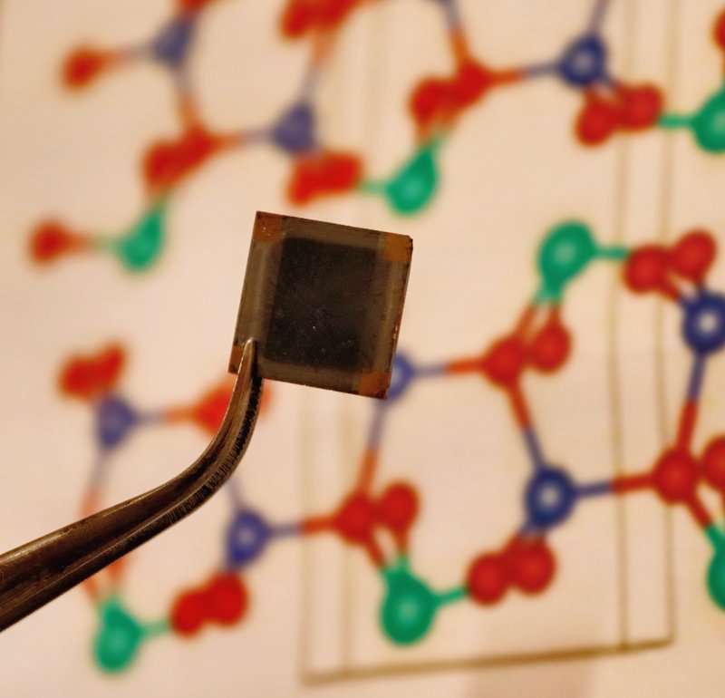
Yuchen Fu, DPhil student in the Hoye Group and experimental co-lead author, commented: “We discovered that CuSbSe2 avoids carrier localisation, which is unusual in emerging solar absorbers based on heavy pnictogens. To unravel the fundamental reasons why, we used a combination of ultrafast spectroscopy and state-of-the-art computational techniques.”
These factors were found to be:
- The presence of regular free volume in the structure, allowing distortions from the propagation of acoustic waves to be relaxed. Carrier localisation takes place because of charge-carriers coupling to vibrations to the structure (phonons). The strength of coupling depends on how much the electronic structure is changed because of the phonon modes. CuSbSe2 has a layered structure, and relaxing these distortions in the inter-layer gaps ensures minimal change to bond lengths, and therefore minimal changes in electronic structure.
- Quasi-bonding between the layers in CuSbSe2. This occurs because each layer is terminated by Sb and Se (and not just Se), such that Sb and Se from neighbouring layers can weakly hybridise. This ensures high electronic dimensionality, which helps to reduce the likelihood of carrier localisation
- Relatively low polarizability of the elements in CuSbSe2 and small bandgap. These result in the dielectric constant having a reduced dependence on frequency, and this contributes to weaker coupling between charge-carriers and optical phonons
Hugh Lohan, another DPhil student in the Hoye Group, and the computational co-lead author, commented: “Early work during this project unexpectedly uncovered the band-like nature of transport in CuSbSe2. Working dynamically with experimentalists, we were able to plan a series of computational probes to aid interpretation of this result and ultimately extract design rules we hope to apply to other materials in the space.”
Professor Robert Hoye, corresponding author on the work, commented: “The principles behind the delocalised charge-carrier transport in CuSbSe2 can be broadly applied. The next step is to test these principles on materials from the wider family of pnictogen-based semiconductors. We are excited by the possibility of making use of the discoveries from this work to enable the design of more efficient solar absorber materials.”
The complete publication can be read in Nature Communications: Y. Fu, H. Lohan, et al. Structural and Electronic Features Enabling Delocalized Charge-Carriers in CuSbSe2 (2024).